


Clicking on the screen shots will expand them to full size.
A Simple Project
The Xilinx Embedded Development Kit (EDK) provides a simple method for creating custom, FPGA based, mixed hardware and software systems. This HowTo will give you a quick guide to getting a basic project up and running.
Note: This HowTo uses Xilinx ISE & EDK version 8.2i
Base System Builder
The first part of any EDK project is the creation of the base system. This describes the hardware on which your software will run. The Base System Builder provides a simple method of specifying your system requirements. Once created, you can load the same base system for other projects.
Stage 1
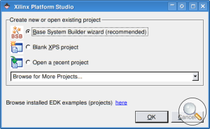
On opening Xilinx Platform Studio (XPS), you will be asked which action you wish to take.
Select Base System Builder wizard and click OK.
Stage 2
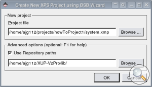
You need to select where the project files will be stored. Use Browse to
select where the system.xmp and other project files will be created.
The Repository path specifies additional locations where EDK can find extra board and IP core definitions. Development boards, such as the XUP-V2Pro board, will have these files available.
For the XUP-V2Pro board, go to http://www.xilinx.com/univ/xupv2p.html
and download the zip file listed as 'EDK Board Definition File (.xbd), Pcores & Drivers'.
Extract this file and specify the location of the lib directory.
Stage 3
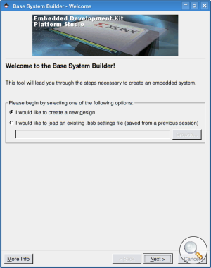
At this point, you have the choice of creating a new design, or selecting a previously specified base system. Select the option to create a new design.
The Base System specifies the type of processor, peripherals and target FPGA. If you've used the Base System Wizard before, you
can use your previous settings if you wish to use the same basic hardware system structure for a new project.
Stage 4
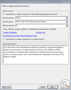
EDK comes with a set of descriptions for various development boards. If you installed the XUP-V2Pro libraries correctly, this should also be available.
Select the following:
Board vendor: Xilinx
Board name: XUP Virtex-II Pro Development System
Board revision: C
If these options are not available you have probably set the wrong repository path in stage 2.
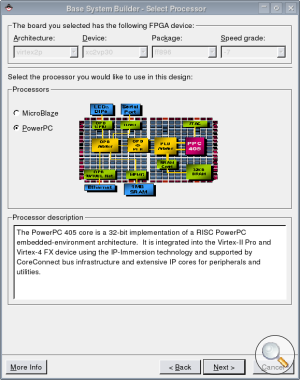
Stage 5
You have a choice of which processor will be at the heart of your embedded design. The Virtex 2 Pro FPGA (XCV2P30) on the XUP-V2Pro board contains two PowerPC (PPC) cores. You also have the option to use the MicroBlaze core.
The PPC is a hard core, using dedicated hardware, the MicroBlaze processor is a soft core and uses the FPGA's configurable resources. The MicroBlaze core allows embedded devices to be created on FPGAs that do not contain PPC hard cores, such as the Spartan range.
Select the PowerPC core.
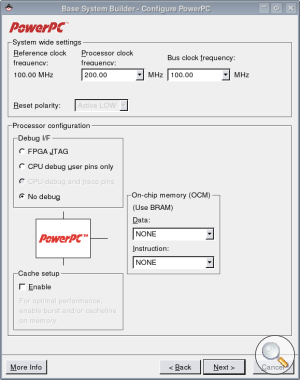
Stage 6
The XUP-V2Pro Board has a number of clock sources. The 100MHz source is used as the main reference clock. You can use the FPGA Digital Clock Managers (DCM) to create alternate clock speeds for your design. For this project, use a 200MHz Processor Clock frequency and a 100MHz Bus Clock frequency.
Make sure the Debug Interface and Memory Cache are disabled.
You also have a choice to use On-Chip Memory for storing data and instructions. The OCM connection to the PPC can speed up your system because both instructions and data use a dedicated bus to the processor. The OCM uses FPGA Block RAM (BRAM), so if you have large memory requirements, you will need to use external memory as well. The XUP-V2Pro board has a SDRAM socket which can be used for external RAM.
Select no On-Chip Memory for this project.
Stage 7
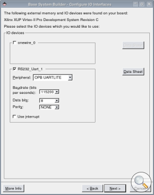
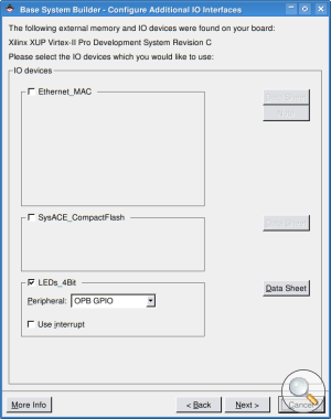
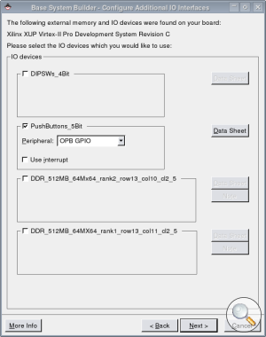
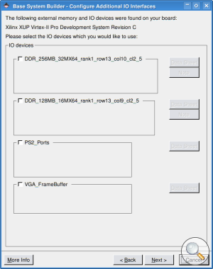
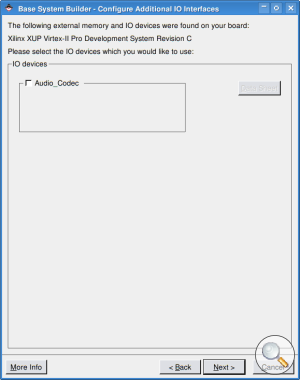
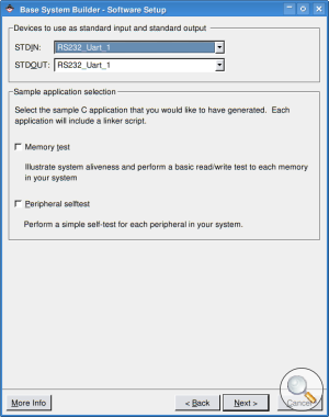
The next set of dialog boxes allow you to include different hardware peripherals in your design. Some are generic, others are specific to the hardware available on the selected development board.
Use the following screen shots as a reference to specify the base system peripherals.
Stage 8
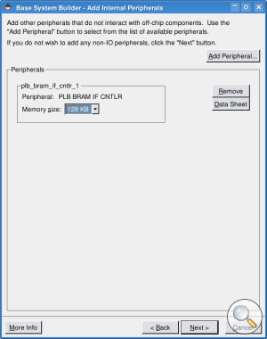
One of the available peripherals is an interface controller to FPGA Block RAM (BRAM). The peripheral shown here uses the PLB (Processor Local Bus) to connect BRAM to the PPC. As we didn't use the OCM in stage 6, we shall use this BRAM to store instructions and data. Select the largest size.
Using FPGA BRAM for storing instructions and data allows your code and initialised variables to be written directly into memory when you configure the FPGA.
Stage 9
The on-board UART can be used as a channel for stdin and stdout. This is
convenient way of transferring data between the FPGA and a PC. It also means you can use printf statements to help debug your code.
XPS can also create a set of test applications. Disable these options.
Stage 10
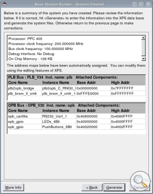
Before generating the base system, you will be reminded of the options you have selected.
Stage 11
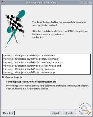
Before finishing the Base System Builder you have the option to save your
settings. The generated .bsb file can then be used again (as in stage
3) to quickly set-up the Base System Builder to settings you have just selected.
Stage 12
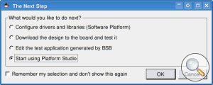
Finally, select the option to start using Platform Studio.
A bsb file with the above settings can be downloaded using the following link:
XPS Interface Overview
Before creating a project, it's worth taking a look at the various parts of the XPS interface. The interface is split into three main sections; a tabbed Platform Information Area panel, the System Assembly View and the Console Window.
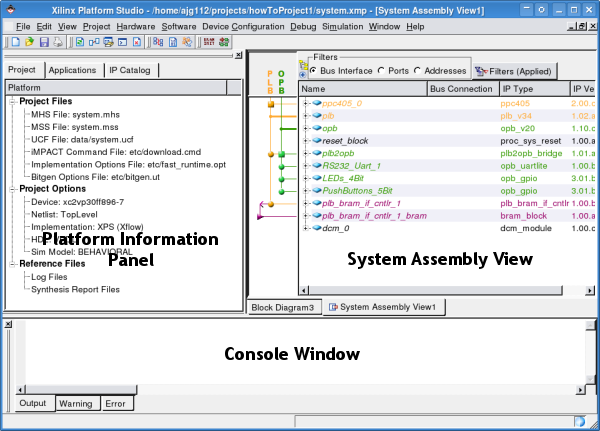
Xilinx Platform Studio
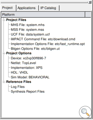
The first tab of the Platform Information Area gives an overview of the system.
system.mhs - This text file describes the parts that make up your system.
system.ucf - This is the user constraint file and describes how signals are connected to the FPGA pins.
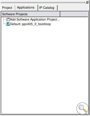
This tab lists your applications. A project can contain multiple applications.
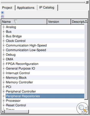
The final tab contains a list of the available peripherals that can be included in your project. This list will also contain custom peripherals of your own design.
Note that some of the listed peripherals are only available under licence, for which you'll have to pay.
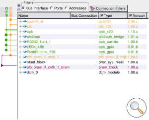
The System Assembly View has three views. The Bus Interface shows how the different peripherals connect to the processor via different busses. The Ports view shows the external connections of each peripheral. The Addresses view shows the memory assignment of the peripherals.
These views will be used in later HowTos when building more complex systems.
System Overview
You can get a visual overview of the system you have created by selecting Project->Generate and View Block Diagram.
The PowerPC is shown at the top in red, this has two connections to the PLB (orange) one is for data, the other for instructions. A bridge is used to connect the PLB to the OPB.
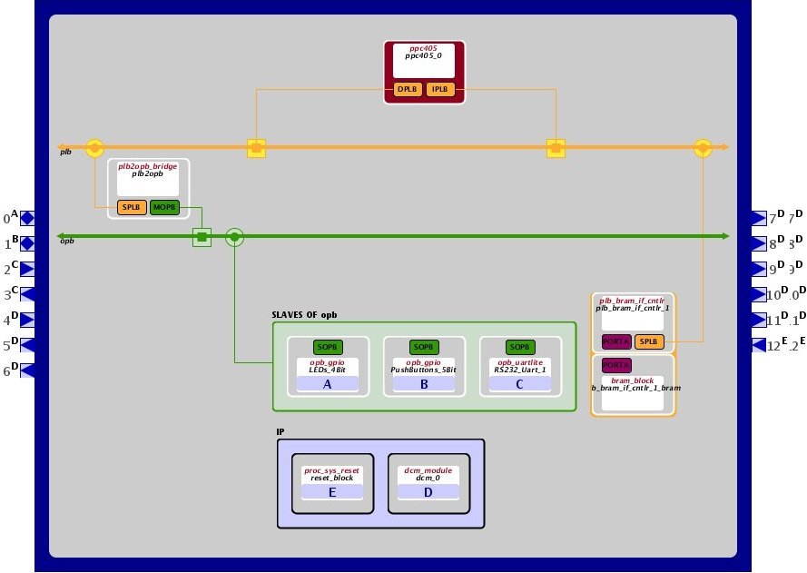
System Block Diagram
A Simple Project
Once you have specified the base system, you can start designing your system.
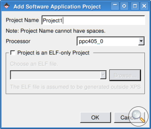
Double click Add Software Application Project... from the Applications tab in the Platform Information Area. Choose a name for your project and click OK.
Note the warning about not having spaces in your project name. This warning also applies to the project path.
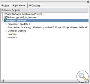
The new project will now be listed, allowing you to specify project options and source files. As you can have multiple applications per project you need to specify which will be configured into the FPGA.
Right click on the Default project and deselect the Mark to Initialize BRAMs flag. Now
right click on the new project and select the Mark to Initialize BRAMs flag.
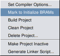
Block RAM initialisation control
All but the required project should have red crosses on their icon. The new project, to be downloaded onto the FPGA, should have a green arrow on its icon.
The next stage is to write the project code. The code listed below polls the status of the board's push buttons and reflects their setting on the LEDs.
ledApp.c#include "xgpio.h" #include "xparameters.h" int main(void) { XGpio gpLED; XGpio gpPB; // Initialise the peripherals XGpio_Initialize(&gpLED, XPAR_LEDS_4BIT_DEVICE_ID); XGpio_Initialize(&gpPB, XPAR_PUSHBUTTONS_5BIT_DEVICE_ID); // Set the LED peripheral to outputs XGpio_SetDataDirection(&gpLED, 1, 0x00000000); // Set the Push Button peripheral to inputs XGpio_SetDataDirection(&gpPB, 1, 0x0000001F); Xuint32 data = 0; while(1) { // Read the state of the push buttons data = XGpio_DiscreteRead(&gpPB, 1); // Set the LED state XGpio_DiscreteWrite(&gpLED, 1, data); } }
To keep all your code together, create a directory within the project
directory called code. Either create a new file using the code
above, or download the file ledApp.c.
Place the finished file into the new code directory.
To add the file, right click on Sources and select Add Existing
Files.... Select the c file.
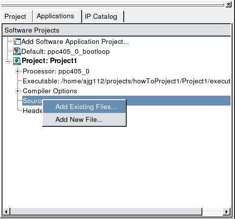
XPS: Adding a new source file
The final stage is to build the system and configure the FPGA. This can be achieved in a single step by selecting Device Configuration->Download Bitstream. You can also use the toolbar button highlighted below. For large projects, this process can take a while. However, this simple example shouldn't take more than 10 minutes (depending on your PC).
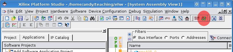
XPS: FPGA Configure
If everything has worked the FPGA should configure and the application run.
The image below shows the buttons and LEDs on the XUP-V2Pro board. If the system has built and configured correctly, pressing the buttons (AH4, AG3, AH1 & AH2) will light the LEDs (AC4, AC3, AA6 & AA5)
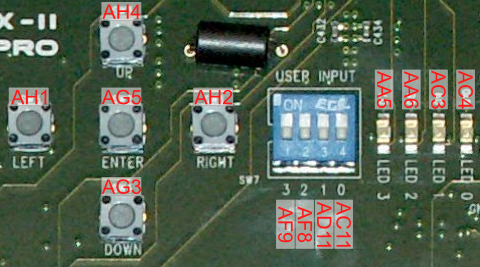
XUP-V2Pro Buttons and Switches
Further Info
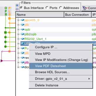
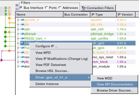
The above project makes use of the XUP-V2Pro Board's LEDs and Push buttons. These are connected to the PPC processor via two General Purpose Input/Output (GPIO) Interfaces. The GPIO peripheral, as the name suggests, provide a basic IO connectivity. Further details on the GPIO Interface peripheral can be found by right clicking on either the LED or Push button listed in the System Assembly View.
|
|
