


VCC VW-300
The VCC VW-300 is a FPGA development board. It has an on board XCV300 Xilinx FPGA. This page contains some details for using the board.
FPGA Pins
The following tables contain the FPGA pin numbers for connections to the board's various peripherals.
|
|
Data Sheets
Below are a set of links to documents related to the board. Included are data sheets for the various components found on the board, board schematics and some articles.
Data Sheets
Schematics
Articles
Test Designs
Below are a set of links to test designs, these could be used as references, or just to check that the hardware is working.
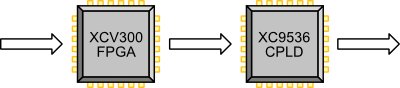
JTAG Configuration Chain
The FPGA on the VCC board can be configured via a JTAG chain. The image below shows the devices on the chain, the Virtex FPGA and a Xilinx CPLD.
JTAG Chain
It is possible, and probably easier, to use impact from the command line. By
using batch files, you can store a set of impact commands. These batch files
are then run by using impact's -batch flag, as shown below. The batch file in
this case being called boardID.batch.
> impact -batch boardID.batch
The batch file shown below will display the contents of the board's JTAG chain and is useful for checking that the cable is all connected up OK.
boardID.batch# Impact batch File # Board ID commands for VCC VW-300 board setMode -bs # Set to Boundary Scan Mode setCable -port lpt2 # Use Parallel port identify # Identify devices info # Display information on devices quit # Quit Impact
This second batch file can be used to configure the FPGA. It reads a bit
file called bitFile.bit. You will also need the BSD file
xc9536.bsd for the CPLD. This can be found within the files installed with ISE.
program.batch# Impact batch File # Program commands for VCC VW-300 board # Program Virtex and bypass CPLD setMode -bs # Set to Boundary Scan Mode setCable -port lpt2 # Use Parallel port addDevice -p 1 -file "bitFile.bit" # Bit File for Vitrex addDevice -p 2 -part "xc9536.bsd" # BSD file for CPLD program -p 1 # Program device 1 - FPGA quit # Quit Impact
