


Evolvable Hardware Lab 2
In this lab you will investigate using a GA for creating a fault tolerant system. You will evolve a set of 4-bit parity generators and place them in a TMR architecture. Faults will be injected into the parity generator circuits and if a failure is detected, evolution will be used to re-evolve the circuits back to full functionality.
Parity Generator
Parity data indicates the numbers of logic '1' bits in a block of data. Parity bits are normally added to the end of a data word to provide a method of detecting alterations in the word's data. The two types of parity bit are even parity and odd parity. When using even parity, the parity bit is set such that the total number of 1s is even. Odd parity is the reverse, the parity bit is set to create an odd number of 1s. The truth table below demonstrates this.
| Input | Output | |||||
|---|---|---|---|---|---|---|
| Hex | D3 | D2 | D1 | D0 | Odd | Even |
| 0 | 0 | 0 | 0 | 0 | 1 | 0 |
| 1 | 0 | 0 | 0 | 1 | 0 | 1 |
| 2 | 0 | 0 | 1 | 0 | 0 | 1 |
| 3 | 0 | 0 | 1 | 1 | 1 | 0 |
| 4 | 0 | 1 | 0 | 0 | 0 | 1 |
| 5 | 0 | 1 | 0 | 1 | 1 | 0 |
| 6 | 0 | 1 | 1 | 0 | 1 | 0 |
| 7 | 0 | 1 | 1 | 1 | 0 | 1 |
| 8 | 1 | 0 | 0 | 0 | 0 | 1 |
| 9 | 1 | 0 | 0 | 1 | 1 | 0 |
| A | 1 | 0 | 1 | 0 | 1 | 0 |
| B | 1 | 0 | 1 | 1 | 0 | 1 |
| C | 1 | 1 | 0 | 0 | 1 | 0 |
| D | 1 | 1 | 0 | 1 | 0 | 1 |
| E | 1 | 1 | 1 | 0 | 0 | 1 |
| F | 1 | 1 | 1 | 1 | 1 | 0 |
You will be creating a fault tolerant circuit implementing the above 4-bit parity generator truth table.
A Cell Array with Fault Injection
The cell and cell array designs used in this lab have been modified from those used in Lab 1. The cell circuit is shown below. The main differences from the previous design are the reduction in size of the LUT and the inclusion of a failure injection multiplexer. The choice of failure mode is set by the 2-bit Fail Mode register. The different failure modes are described in the table below.
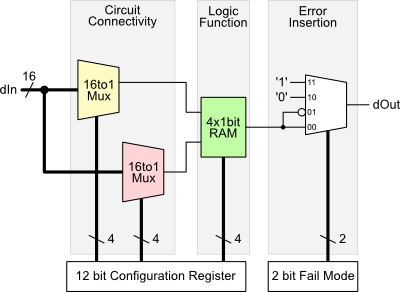
Fault Tolerance Cell |
|
The cell now has 12 configuration bits due to the removal of one input connection multiplexer and the reduction in LUT size. Their order and function is shown in the figure below.
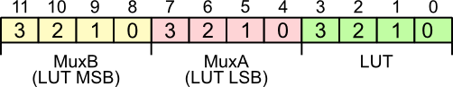
The Configurable Cell Config bits
Cell Array
The new Cell Array uses 32 cells in a 4 by 8 grid. The interconnections between the cells are different from the previous lab. As before, each cell has a 16-bit input, but this time the bus is created from different sources. Each cell has a connection to the 4-bit input (red) and an inverted copy of this input (blue). The remaining 8 bits are made out of the outputs from the cells of the previous column (orange). For the special case of the first column, these 8 bits are held at '0' (green).
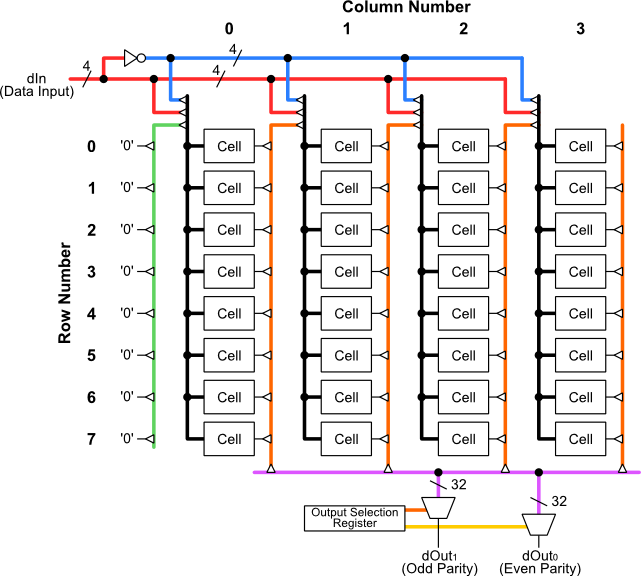
The Fault Tolerance Cell Array
The cell array outputs can be taken from any cell in the array. The output
selection multiplexers are connected to all 32 cell outputs (purple). The two array outputs, dOut1 and dOut0
are derived from these 32 signals. The configuration bits for the output selection multiplexers
are shown in the figure below. 5 selection bits are required per output
(25=32).
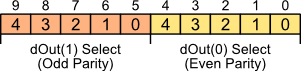
The Cell Array Output Selection Register
| Total number of configuration bits | = (# cells * # cell configuration bits) + (# outputs * # output selection bits) |
| = (4 * 8 * 12) + (2 * 5) = 394 bits |
The cell array structure has been altered to improve the circuit's ability re-evolve solutions after a fault has been injected. Think why this is the case.
The FTBlock
Three cell arrays are enclosed in a block called FTBlock. The structure of
this block is very similar to the EvoBlock used in the previous lab, except
this time there are three rather than eight cell arrays. The structure of the
FTBlock is shown in the figure below (at the moment you can ignore the
circuitry in grey).
As before, there is a RAM block to hold the target truth table, and a set of xnor gates for calculating the match between the RAM outputs and the cell array outputs. The mask register function has been removed as we shall always be making use of all (both) cell array outputs.
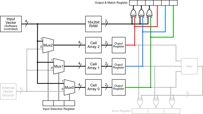
Fault Tolerance System 1
The format of the FTBlock Output & Match register is shown below.
Cell Array Output Register
Triple Modular Redundancy
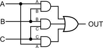
Triple Modular Redundancy (TMR) is static redundancy architecture. It provides a method for masking faults in a system. The left-hand figure below shows the TMR architecture. Three functionally identical units are used in parallel. A voter unit is used to generate a single output that is a majority vote of the three system outputs. Therefore, if a single unit fails, the two others will out vote it, and the voter output remains correct. The right-hand figure shows the circuit for a voter.
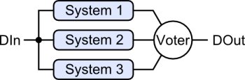
TMR System |
Voter Circuit |
The figure below shows the full FTBlock circuit. You should be able to see
the TMR architecture within this circuit. The outputs from the three cell
arrays are connected to a voter. A set of three xor gates, labelled
Discrepancy Detection, are used to indicate the failure of a cell
array to output the correct parity data with respect to the voted output.
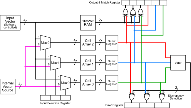
Fault Tolerance System 2
Using this setup, the overall lab aim is to achieve the following:
- Set the vector source to the software controlled input vector
- Evolve three working Parity Generators
- Switch to the internal vector source (purple)
- Inject an error into a Cell Array
- Detect which Cell Array has failed
- Switch to the software controlled vector source
- Re-evolve the failed Cell Array (to remove, or make use, of the fault)
- Switch to the internal vector source
- Go back to 3
Creating the System
The full hardware system and a software shell have been setup for you. The project files can be downloaded using the link below (refer to the previous lab if you've forgotten how to open up the project). Remember, you will probably have to use local temporary storage space to unpack the project to avoid disk quota issues.
The file that needs completing is exp1.c, this can be found in the project's code directory. The areas requiring attention are commented with a TODO flag. The following sections will guide you through filling these sections. The Function Reference provides extra information.
Loading the Target Truth Table
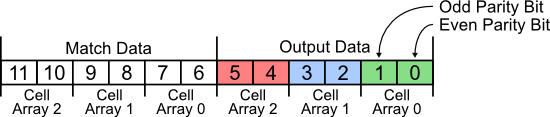
As before, you need to load in a truth table for the target circuit into the RAM block. The format for the RAM word is shown below. Bit 1 holds the odd parity bit and Bit 0 the even parity bit.

RAM Format
Look for the following function:
void loadTargetTruthTable()
Fill this function with the code to load the correct data. You will need to use the following special macros:
FTBLOCK_writeVector(data)
- This macro applies an input vector to the FT Block and sets the look up address for the Target RAM.FTBLOCK_writeTargetRAM(data)
- This macro loads the location in Target RAM pointed to by the applied vector. Note, that calling this macro automatically increments the vector value.
When you have filled the function, compile and download the design. The
target RAM will be loaded using your function, then the contents will be
retrieved and output over the serial port. Check this output to see if your
loadTargetTruthTable function has worked correctly.
When the target RAM is being loaded correctly, comment out the return statement labelled STOP1 and continue.
Fitness Function
Completing the GA requires a number of tasks. The first is to create the fitness function. The function prototype is shown below. This function needs to calculate an individual's fitness from the match data passed to it. As before, a '1' represents a match and a '0' a difference in output.
The match data passed to this function is for a single cell array. The value is 2 bits, shifted towards the LSB.
Xuint32 calcFitness(Xuint32 matchData)
You also need to calculate what the maximum fitness is for the parity generator. Set the define MAX_FITNESS to this value.
#define MAX_FITNESS ??
Mutation Operator
You need to write a mutation function for this system. The prototype of the mutate function is shown below. Again, search for the TODO to see where you should add your code.
void mutateArrayConfig(ArrayConfig *source, ArrayConfig *dest, Xuint32 mutationRate)
As before, the configuration for a complete cell array is held in the
ArrayConfig structure. This structure is declared in the ftBlock.h
file. Spot the addition of the members for the output selection configuration. You
will need to take these into account when writing your mutation function.
ftBlockCtrl.htypedef struct { Xuint32 cellConfigs[NUM_CELLS]; Xuint32 outputSel0; Xuint32 outputSel1; Xuint32 fitness; } ArrayConfig;
Evolve Function
For this lab, the job of evolving a solution is enclosed within a single
function, findSolution. This allows us to call for a new working
configuration on demand. The function prototype is shown below. The arrayNum
argument is the number of the cell array that should be used for evolution.
Only a single array is used so the functionality of the others is not
disrupted. The function returns a success value, 0 if a working
solution was found, 1 if no solution was found.
Xuint32 findSolution(Xuint32 arrayNum)
A basic GA has already been written within the findSolution
function.
Once you have written your calcFitness function, calculated the
MAX_FITNESS and written your mutateArrayConfig function,
compile your code and configure the FPGA. The code will try to find three
working parity generator solutions, one for each cell array. If this succeeds,
comment out the return statement labelled STOP2.
Fault Injection
You should now have a system that uses a simple GA to evolve a working parity generator within each cell array. After configuring the FPGA, if three solutions are found, you will receive the following prompt:
Ready for fault injection
Three of the development board's switches can be used to inject faults into the cell arrays. Press one of the buttons indicated in the figure below. The fault location and type will be output over the serial port. If the fault has caused a cell array failure, the corresponding LED will light and the system will attempt to re-evolve a solution.
Note: It is possible to inject a fault and not cause a failure. This occurs if the fault is injected into a cell that is not being used by the current evolved solution. However, when re-evolution is triggered, all the faults injected so far will still be present.
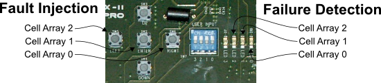
XUP-V2Pro Buttons
Things to Try
Once you have the basic system running, there are two areas to investigate further. The first is to improve the speed of the GA's convergence to a solution, thus making recovery as quick as possible.
Secondly, try adapting the GA to produce circuits with intrinsic fault tolerance. That is circuits that can accommodate faults without failure. Two approaches can be taken. Try forcing evolution to find solutions that use the minimum number of cells. This will increase the number of failed cells a cell array can take before failure. Or try testing a circuit's resistance to faults during evolution.
Function Reference
Below is a description of the ftBlock.h and ftBlock.c files. These are
used to help with interfacing with the FTBlock module and to perform various
evolutionary tasks.
ftBlock.h
Defines#define NUM_CELLS 32 #define NUM_CONFIG_BITS 12 #define NUM_OUTPUT_SEL_BITS 10
NUM_CELLS defines the number of cells in the array, in this case 4 columns * 8 rows = 32.
NUM_CONFIG_BITS is the number of bits used to configure a cell, in this case 12 bits.
NUM_OUTPUT_SEL_BITS is the total number of bits used to select the cell array outputs.
typedef struct
{
   Xuint32 cellConfigs[NUM_CELLS];
   Xuint32 outputSel0;
   Xuint32 outputSel1;
   Xuint32 fitness;
} ArrayConfig;
The ArrayConfig structure holds the configuration for a complete array. It also has a member to hold the
configuration's fitness. A 32 bit unsigned int is used to hold a cell's config data, however, you'll only
be using the first 12 bits of this data. There is also the outputSel members for holding the output selections, only 5 bits of each is used.
void FTBLOCK_writeConfigArrayNum(Xuint32 data)
This sets the array which will receive configuration data when using the FTBLOCK_writeConfig macro and the output selection data
when using the FTBLOCK_writeOutputSel macro.
void FTBLOCK_writeConfigCellNum(Xuint32 data)
This selects where a cell configuration is written to when using the FTBLOCK_writeConfig macro. Note
that the cell number is automatically incremented when FTBLOCK_writeConfig is called.
void FTBLOCK_writeConfig(Xuint32 data)
This writes configuration data to the cell selected with the
FTBLOCK_writeConfigArrayNum and FTBLOCK_writeConfigCellNum macros. Note
that calling this macro automatically increments the cell number.
void FTBLOCK_writeOutputSel(Xuint32 data)
This writes the output selection to the array selected with
FTBLOCK_writeConfigArrayNum macro. Both selections are written at once. The
data format is shown below.
| 9-6 | Output Selection 1 |
| 5-0 | Output Selection 0 |
void FTBLOCK_writeFailModeArrayNum(Xuint32 data)
This selects the array which will receive the fail mode settings using the FTBLOCK_writeFailMode macro.
void FTBLOCK_writeFailModeCellNum(Xuint32 data)
This selects the cell which will receive the fail mode settings using the FTBLOCK_writeFailMode macro.
void FTBLOCK_writeFailMode(Xuint32 data)
This writes a failure mode to the cell selected with the FTBLOCK_writeFailModeArrayNum and FTBLOCK_writeFailModeCellNum. The
fail modes are shown below.
| 0 (00) | No fault, the cell output is unaltered. |
| 1 (01) | The LUT output is inverted before leaving the cell. |
| 2 (10) | Stuck-at-0, the cell output is held at '0'. |
| 3 (11) | Stuck-at-1, the cell output is held at '1'. |
void FTBLOCK_writeInputSel(Xuint32 data)
This sets which vector source will drive the cell arrays. The source may be an internal counter or a vector written under software control. There is a selection bit per cell array. Bits 2 to 0 select arrays 2 to 0 respectively. A value of 1 selects the external (software controlled) source, and value of 0 selects the internal vector source.
void FTBLOCK_writeVector(Xuint32 data)
Write a vector to the cell arrays. Whether the vector is actually applied to
the cell arrays depends on the input selection settings set using the
FTBLOCK_writeInputSel macro.
void FTBLOCK_writeTargetRAM(Xuint32 data)
This writes a value to the target RAM at the address pointed to by the vector value set with the FTBLOCK_writeVector macro.
Note that calling this macro automatically increments the vector value.
void FTBLOCK_resetError(Xuint32 data)
This resets the error flags that are set when a discrepancy is found between a cell array's output and the other two array outputs.
Xuint32 FTBLOCK_readConfigArrayNum()
Read the current array number selected for configuration.
Xuint32 FTBLOCK_readConfigCellNum()
Read the current cell number selected for configuration.
Xuint32 FTBLOCK_readFailModeArrayNum()
Read the current array number selected for fail mode injection.
Xuint32 FTBLOCK_readFailModeCellNum()
Read the current cell number selected for fail mode injection.
Xuint32 FTBLOCK_readInputSel()
Read the input selection bits.
Xuint32 FTBLOCK_readVector()
Read the current vector applied to the cell array. Whether this is the value
actually applied to the cell arrays depends on the input selection settings set
using the FTBLOCK_writeInputSel macro.
Xuint32 FTBLOCK_readTargetRAM()
Read the contents of the target RAM currently pointed to by the vector set using the FTBLOCK_writeVector macro.
Xuint32 FTBLOCK_readOutputMatch()
Read the output and match data from the three cell arrays. The format of this data is shown below. Note for each bit pair, the MSB corresponds to the odd parity bit and the LSB to the even parity bit.
| 11:10 | Match data from cell array 2 |
| 9:8 | Match data from cell array 1 |
| 7:6 | Match data from cell array 0 |
| 5:4 | Output data from cell array 2 |
| 3:2 | Output data from cell array 1 |
| 1:0 | Output data from cell array 0 |
Xuint32 FTBLOCK_readError()
Read the error flags that are set when a discrepancy is found between a cell array's output and the other two array outputs.
ftBlock.c
Functionsvoid configureArray(Xuint32 arrayNum, ArrayConfig *config)
Configure a whole array. Note that a pointer is used to pass the config data to the function.
void randomiseArrayConfig(ArrayConfig *config);
Randomises the array configuration passed to the function. Note that a pointer is used to pass the config data to the function.
