


Clicking on the screen shots will expand them to full size.
Simple Nios II System
This HowTo describes creating a simple embedded processor system using Altera FPGA tools. You can use any Altera FPGA development board, although the howto does include a simple UART, so a serial port is helpful.
Note: This howto is based on Quartus II Web Edition v11.1 (The service pack is important for correct operation).
Setting up the project
Start Altera Quartus
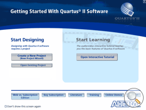
Start Altera Quartus II, this is the main FPGA development application. The application icon is shown below.
The welcome screen is shown to the left, click the 'Create New Project' button.
Project Location
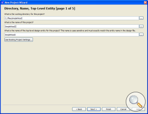
Click 'Next' to take you to the first proper page of the 'New Project Wizard'. Page 1 is used to name the project and set where the project files will be held.
Create a new folder and enter it's location in the first text field of the window. Enter the
project name 'SimpleNiosII' in the second text field, the third field will automatically filled in.
The completed form is shown to the left.
Select FPGA device
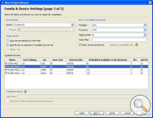
Skip past the second window to the third. Select the FPGA device that is being targeted.
Press Finish
Creating the embedded System with Qsys
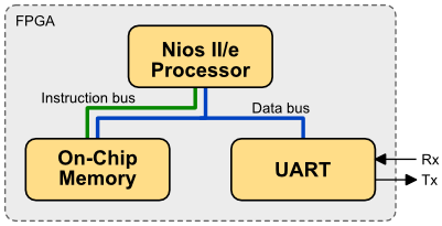
Qsys is Altera's 'System integration tool', it is used to create the embedded system by bolting together modules such as processors, memory blocks and communication peripherals.
The system that will be created for this HowTo is illustrated below.
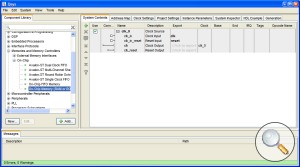
Start Qsys
Start Qsys from the Quartus II menu. Tools » Qsys
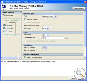
Add On-Chip Memory
The first module to add is some memory, this is used to hold both the instructions and data used
by the processor. From the Component Library select Memories and Memory
Controllers » On-Chip » On-Chip Memory (RAM or ROM),
then click the add button. As the name suggests, On-Chip memory, is memory
located within the FPGA itself, rather than an external memory devices.
The memory configuration window will appear, change the Total memory size to 8192
Bytes (8KB), then click finish. This is actually far more than is required for this HowTo, but gives
plenty of space for later projects.
To rename the memory module, single click on it's current name 'onchip_memory2_0, press F2, then rename to 'memory'
The errors and warnings in the messages window can be ignored at this stage
Add Nios II/e
The next step is to add a Nios II core. From the Component Library select
Embedded Processors » Nios II Processor, then click the add
button.
The configuration window offers a choice of three cores. Select the Nios II/e core, this is the 'economy' core, the others require a licence.
Select the 'JTAG Debug Module' tab and select 'No Debugger'. By deselecting the debugger you will not be able to load code into the processor via JTAG or debug the running processor. However, neither is necessary for simple projects. Using on-chip memory means the processor's instructions and data can be stored in the FPGA configuration file and therefore are ready as soon as FPGA configuration is complete..
Click finish and rename the processor to 'cpu'.
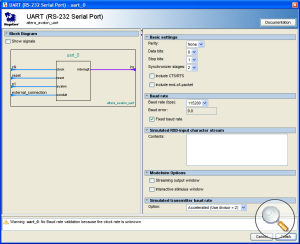
Add UART
From the Component Library select Interface Protocols »
Serial » UART (RS-232 Serial Port), then click the add
button.
Set BAUD rate to 115200, click finish and rename the module to 'uart'
The UART data lines need to be exported so they can be connected to the FPGA's pins. The export column
within the main Qsys window allows external connections to be made. Click on 'Click to export' on
the UART's external_connections row. Enter the name 'serial' and press
enter.
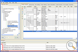
Connect Modules
All the modules need to be connected together, this is achieved by clicking on nodes within the connections column.
First connect the clock and reset signal to each module. Next connect the
CPU's data_master and instruction_master to the memory 's1'
port. Finally, connect the CPU's data_master to the UART.
The screen shot on the left shows the completed connections.
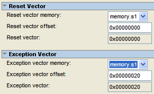
Select CPU Memory and Assign Addresses
Now that the Nios II core has memory attached to it, it is possible to assign the processor's
reset, exception and break vectors. Double click the Nios II module. In the first tab of the configuration
window there are two sections labelled 'Reset Vector' and 'Exception Vector'. For both, select the
memory 'memory.s1' from the selection box, leave the offset values as they are.
Select the 'JTAG Debug Module' tab, in the 'Break Vector' section, select the memory
'memory.s1' from the selection box. Now click Finish.
Now the base addresses of each module needs to be set, this can be done automatically by
selecting System » Assign Base Address from the menu of the main
Qsys window.
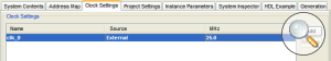
Clock
The frequency of the clock driving the embedded system needs to be specified. The frequency can be set selecting the 'Clock Settings' tab. Double click the value under the 'MHz' column and enter the correct frequency. In this case the input clock frequency has been set to 25MHz.
It is likely that required setting is the frequency of the clock source connected to the FPGA.
Save and Generate
The last step in Qsys is to save the system and generate the HDL that describes the system. Select
Files » Save, browse to the project's directory, enter
'HostSystem.qsys', and click 'Save'.
Now select the 'Generation' tab and click 'Generate'.
Don't worry about warnings. When finished, click close.
If there are any problems try downloading and opening the Qsys file linked to below.
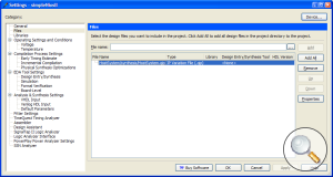
Add to Quartus II Project
The generated system now needs to be added to the main project. In Quartus II, select
Project » Add/Remove Files in Project.... The Settings window will
appear, select the browse button (three dots) at the end of the File Name text box. In the
Select
File
window, change the Files of type filter to All Files
(*.*). Navigate to the project directory, then into HostSystem/synthesis.
Select the HostSystem.qip file and click Open. Back in the Settings window, click Add
then OK.
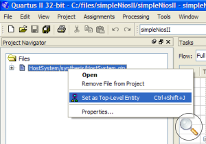
Set Top Level Module
Quartus needs to be told which module represents the top of the design hierarchy. For this simple
design, this is simply the Qsys system that has just been added to the project. In the Quartus
'Project Navigator' window, select the 'Files' tab. Right click on
HostSystem/synthesis/HostSystem.qip and select 'Set as Top-Level Entity.
Creating a Board Support Package
The board support package is a collection of code specific to the system generated by Qsys. It provides APIs that provide access to the system's peripherals and header files that describe the system.
Start NIOS II Software Build tools, this can be done from the Quartus menu Tools »
Nios II Software Build Tools for Eclipse. Alternatively, the icon is shown below
If not run before, you'll be asked for a 'workspace' location, select the default, nothing much is stored in there.
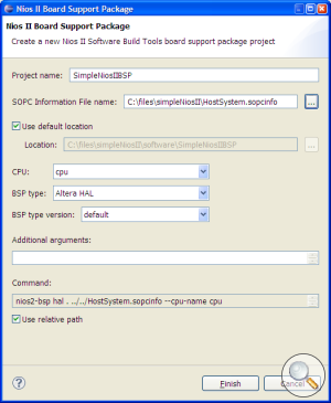
New BSP
To create a new BSP, select File » New » Nios II
Board Support Package.
Change the 'Project name' to SimpleNiosIIBSP. The SOPC Information File
(HostSystem.sopcinfo) can be found in the project directory. The other fields can be left as they are. Click 'Finish'.
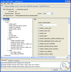
BSP Configuration
First make sure 'SimpleNiosIIBSP' is selected in Eclipse's 'Project Explorer' panel.
Select Nios II » BSP Editor... from the menu.
When the BSP editor has started, in the left hand panel, select the top of the settings tree labelled 'Settings'. This ensures all settings are visible in the right hand panel. Next, make sure that the only ticked boxes enabled are those listed below.
These settings will result in the smallest application binary size at the expense of higher level functionality. Click 'Generate', then 'Exit'.
Build the BSP
Finally, select Project » Build Project from the menu.
Writing a Simple Application
It is now possible to write a simple application to run on the Nios II processor. The instructions below will result in a simple programme that will output a string from the UART.
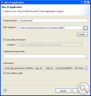
Create an Application
To create a new application, select File » New » Nios
II Application from the menu.
Set the project name to SimpleNiosII (although it can be anything you like). Set the
'BSP Location' to SimpleNiosIIBSP (Use the browse buttons to get a list of available
BSPs). Click 'Finish'.
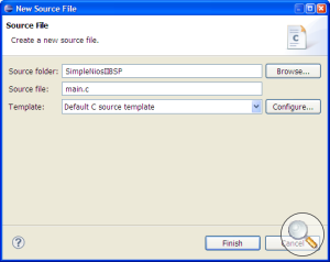
Add a Source File
To add a new source file, right click 'SimpleNiosII' (from the 'Project Explorer'
panel) and select New » Source File.
Enter main.c in the 'Source file' text box and click Finish.
Write The code
The application code is listed below, there is also a link to a source file to download. This simply outputs a string of characters to the UART. Take a look at the Altera Embedded Peripherals IP User Guide to find out the register map for the UART peripheral.
main.c#include <stdint.h> #include "system.h" int main(void) { volatile uint32_t *uart = (volatile uint32_t*) UART_BASE; char *str = "Hello from NIOS II\n"; while (1) { char *ptr = str; while (*ptr != '\0') { while ((uart[2] & (1<<6)) == 0); uart[1] = *ptr; ptr++; } } return 0; }
Build and Create a Hex File
The application can now be compiled. Select Project » Build
Project. The compilation should produce a programme size of about 400 Bytes, the program size
will be printed towards the bottom of the console log. If it is much larger double check BSP
settings.
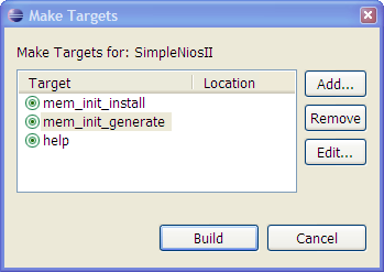
The last stage is to generate a memory initialisation hex file of the application binary. This
will be merged into the FPGA configuration file such that the on chip memory is initialised with the
application instructions and data. To generate the hex file right click 'SimpleNiosII',
select, Make Targets » Build.... Double click
'mem_init_generate'
Add Hex File to Project
Quartus needs to know where to find the hex file so it can be merged with the final configuration
file. Within Quartus select Project » Add/Remove Files in
Project.... The Settings window will appear, select the browse button (three dots) at the end
of the File Name text box. In the Select File window, change the
Files of type filter to All Files (*.*). Navigate to the project
directory, then into software/SimpleNiosII/mem_init, select meminit.qip
and click open. Back in the Settings window, click Add then OK.
Adding Time Constraints
The FPGA tools need some information about the design to know if it's timing meets the capabilities of the FPGA device. For this simple design, we just need to provide information about the clock connected to the FPGA.
Create the file listed below or download from the link and save it to the root of the FPGA
project, the suggested filename is SimpleNiosII.sdc. The file specifies and external
clock with a period of 25MHz.
This file also needs to be added to the project. Within Quartus select Project
» Add/Remove Files in Project.... The Settings window will appear, select the
browse button (three dots) at the end of the File Name text box. In the Select
File window, change the Files of type filter to All Files (*.*).
Navigate to the project directory and select the file and click Open. Back in the Settings window,
click Add then OK.
SimpleNiosII.sdc# Create Clock # ------------ create_clock -name {clk} -period 40.000 -waveform { 0.000 20.000 } [get_ports {clk_clk}] derive_clock_uncertainty
Pin Placement and Compilation
The connections between the internal FPGA fabric and the FPGA's external pins needs to be defined. However, the Quartus tools first need to analyse the design to find what top-level connections are defined and are available for connection to pins.
From the Quartus menu, select Processing » Start » Start Analysis and
Elaboration. All being well, this should complete without any errors.
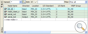
Now the pins can be assigned. Start the Pin Planner from the menu, Assignments » Pin
Planner. It is now a simple job of dragging the Nodes from the list onto the pins of the FPGA
diagram. It is also a good idea to set the I/O Standard for each pin; find the column labelled I/O
Standard in the nodes table and change to the appropriate standard (probably 3.3-V LVTTL).
It is worth checking what Quartus will do with unused pins and what it considers to be the default I/O standard.
Select Assignments » Device... from the Quartus menu. Then click the button labelled Device and Pin Options.
- Select 'Unused Pins' and change 'Reserve all unused pins' to 'As input tri-stated with weak pull-up'.
- Select 'Voltage' and change 'Default I/O Standard' to what is appropriate (probably 3.3-V LVTTL).
Compilation
It is now finally possible to compile the design and generate a configuration file with which to programme the FPGA. Select
Processing » Start Compilation from the menu.
Configuration and Testing
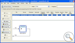
The FPGA programming tool can be started from the Quartus menu: Tools »
Programmer. Click the Hardware Setup button, and select the programming cable.
Then click start in the main programmer window. If everything has worked there should be a stream of
messages being output over the serial port.
Making Changes
After making changes to the software, use the steps below to update the configuration file.
- Recreate the hex file, see Build and Create a Hex File
- In Quartus select
Processing » Update Memory Initialization File - Then select
Processing » Start » Start Assembler - Reconfigure, see Configuration and Testing
When hardware changes are made, such as changing the embedded system structure in Qsys, the
design needs to be recompiled as described in Compilation. Changes in
Qsys will probably also require the Board Support Package to be updated. Within the Software Build
Tools, right click SimpleNiosIIBSP within the Project Explorer and select NIOS II
» Generate BSP
